
17. Ceramic Thick and Thin Film Circuits
| 1903 Page: 410 of 418 Go To Page: | ◁◁ First | ◁ Previous | Next ▷ | Last ▷▷ |
IBM used an early version of this technology in its computers in the 90’s. They used four-inch square sheets that were cut from a green roll of alumina-based tape and many interconnection holes of 150 micron diameter were punched in predetermined positions. Molybdenum-based ink was used to print conductive line patterns 100 micron wide and spacing, and to fill the via holes. The sheets were then pressed together and sintered in a reducing atmosphere (to protect the molybdenum) at 1400 - 1600 ºC. The final structure was 90 x 90 x 5 mm with 33 layers of buried circuitry.
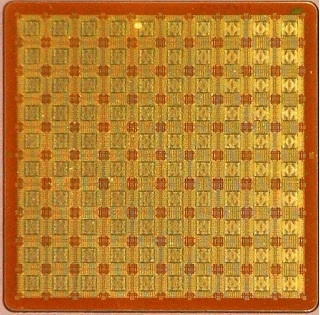
IBM’s 61-layer LTCC 1992
- source Rao Tummala
One problem of using alumina as a substrate is that a refractory metal such as molybdenum or tungsten has to be used as the conductor, but they have a relatively high resistivity. Unfortunately conventional conductive metals oxidise under the high-firing conditions required for sintering alumina, so cannot be used. The increased resistance of refractory metals is a particular problem at microwave frequencies. Also the refractory metals have to be plated to permit subsequent soldering. To overcome these problems, conductive ceramics are often used in thick film circuits. An example is the ceramic conductor, bismuth rubidium oxide, which is also used in fuel cells, high energy density batteries, electrochromic windows, gas separation membranes and automobile exhaust sensors.
Another way of overcoming the problem of incompatibility of these high temperature co-fired ceramics (HTCCs) and high conductivity metals, such as copper and silver, is to use lower firing ceramics. This is achieved by using tailored glass ceramics that can be sintered at between 850 and 1050 ºC. They are used today in multi-layer and multichip modules. The cast tape is initially a glass that has the silver, gold or copper circuitry as well as other materials printed on it to form each layer separately. Between 6 and 50 layers are then laminated, typically using 3000 psi at 70 ºC for 10 minutes, and then sintered, when the additives in the glass cause it to de-vitrify into a glass ceramic. The structures are known as low-temperature co-fired ceramics (LTCCs).
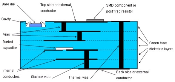
Diagram of LTCC structure - source Sunlord
In a complex circuit there can be hundreds or even thousands of embedded components. Ferrites can be integrated into low temperature co-fired ceramic structures, as spirals for inductance with ferrite layers top and bottom. They can also be used for microwave isolators and circulators, using glass-bonded magnetic ceramics (less than 15% glass) based on, for example, nickel zinc copper ferrites. Active chips are subsequently added to the surface of the LTCC package.
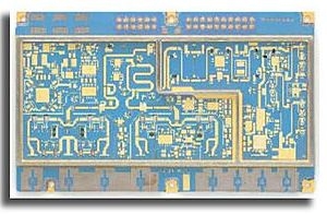
LTCC filter - source cmag technology
With the increased complexity and miniaturisation of equipment such as mobile phones with “Bluetooth” technology containing several hundred capacitors and resistors, even surface mount technology is stretched. Also the number of solder joints becomes so high that reliability suffers. The solution is proving to be fully integrated three-dimensional ceramic packages based on LTCCs. However, LTCC have somewhat inferior mechanical and thermal properties compared with HTCC.
| Page: 410 of 418 Go To Page: | ◁◁ First | ◁ Previous | Next ▷ | Last ▷▷ |
Author: Dr. Stan Jones © Copyright 2010 -